Samsung S7 Edge Circuit Diagram
Samsung t-con board schematic diagram pdf Samsung schematic j2 diagrama 6s схема wiring schematics инструкция s5 duos danny Samsung pdf schematics and diagrams
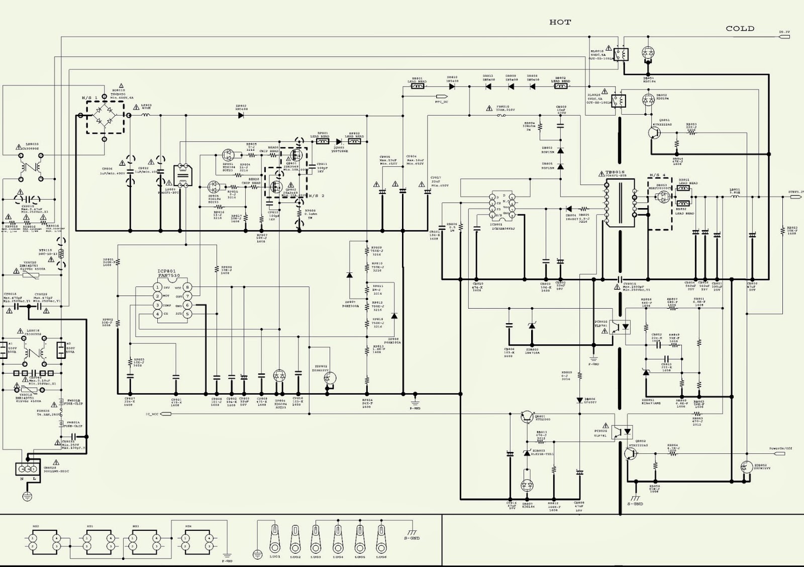
samsung circuit diagram - Circuit Diagram
Samsung galaxy s5 circuit diagram S7 diagram edge samsung galaxy Samsung galaxy s7 circuit diagram
Edge s6 samsung solution galaxy charging paused jumpers diagram charger repair choose board u2ugsm
S7 edge g935f schematics pdf đồ sơSamsung s7 edge schematic diagram Samsung schematic diagram pdfSamsung s7 edge schematic diagram.
Samsung g935f s7 schematicSamsung s7 edge schematic diagram Samsung galaxy s6 edge, galaxy s6 edge, galaxy s6Samsung galaxy s7 edge sm-g935f schematic diagram service manual.

Galaxy schematic g935f sm
S6 schematics g925S7 schematic [get 30+] galaxy s6 schematic diagram download[get 30+] galaxy s6 schematic diagram download.
Samsung s7 edge circuit diagramSamsung galaxy s6 circuit diagram S7 charging g935f problem lcd oppo recognizedSchematics s7 galaxy schematic smartphone manualsonline mobilephone manuals.

38 samsung galaxy s7 diagram
Pin on hardwaerSamsung pdf schematics and diagrams Pin on repairGalaxy s5, samsung galaxy s6, simple code, hard to find, diagram.
S7 samsung g935f edge ways jumper charging galaxy usb problem solution jack headphone hands not ringer u2ugsmSamsung galaxy s7 edge sm-g935f schematic diagram service manual Phone pcb diagram mobile samsung parts smartphone galaxy part motherboard board s7 components sm phones schematic layout circuit iphone flashSamsung galaxy s7 edge sm-g935f schematics.
Samsung s7 edge schematic diagram
Samsung circuit diagramSamsung galaxy s6 edge plus repair schematic S6 repairxSamsung s7 circuit diagram.
Samsung galaxy s7 circuit diagramSamsung galaxy s7 edge teardown Solved: diagram for samsung galaxy s7 edge (g935f)S7 samsung galaxy edge teardown sensor fingerprint myfixguide remove.

Samsung galaxy s7 g935f charging problem ways solution
Samsung galaxy s7 edge sm-g935f schematicsSamsung s7 circuit diagram Samsung s7 schematic diagramSamsung s7 schematic diagram.
Mobile phone pcb diagram with partSamsung galaxy s7 edge g935f usb charging problem solution jumper ways .


SAMSUNG GALAXY S7 EDGE SM-G935F SCHEMATIC DIAGRAM Service Manual

Samsung Galaxy S7 edge G935F Usb Charging Problem Solution Jumper Ways

Samsung galaxy s6 edge, Galaxy s6 edge, Galaxy s6

Samsung PDF Schematics and Diagrams - Schematic diagrams, User's

Mobile Phone PCB Diagram With Part | Mobile Repairing Online
![[Get 30+] Galaxy S6 Schematic Diagram Download](https://i2.wp.com/appleunlockstore.com/images/gallery/Manuals/G920F.jpg)
[Get 30+] Galaxy S6 Schematic Diagram Download

38 samsung galaxy s7 diagram - Wiring Diagram Images